
1. Eight Major Steps to Semiconductor Fabrication
Semiconductor manufacturing process is basically to create patterns on thin films and to create devices that embody functions that are intended in three-dimensional structures as these patterns are stacked on top. To do this, the membrane needs to be stacked, patterned and carved, and another material filled in it. This series of processes is called semiconductor manufacturing processes, and Samsung Electronics’ Job Description standards include Photo, Etch, CVD Metal, Diffusion Implant, CMP, Clean 8 unit processes, including wafer production, and EDS and packaging. In fact, the eight major steps are classified according to the current manufacturing technology, which may add additional processes as the technology advances. Anyway, the important thing is that semiconductor manufacturing processes repeat each of these unit processes to manufacture chips with the desired structure.
2. Front-End Process and Back-End Process
The process of manufacturing chips is divided into Front-End Process and Back-End Process. Front-End Process is a process of manufacturing chips on wafers and testing them so that functions can be performed through the unit process, and Back-End Process is a process of packaging and attaching them to various electronic devices. In [Fig. 1-1], Front-End Process means step 2 and post-process 3 to 5. A is divided into FEOL (Front-End-Off-Line) and BEOL (Back-End-Off-Line), and MOL (Middle-Off-Line) is added in the middle. FEOL mainly includes processes such as Gate/Source/Drain, which are classified as necessary for the manufacture of devices. Since then, MOL is a process that creates a plug that connects electrical contact and wiring of each terminal, and BEOL refers to a wiring process[Fig. 1-2].
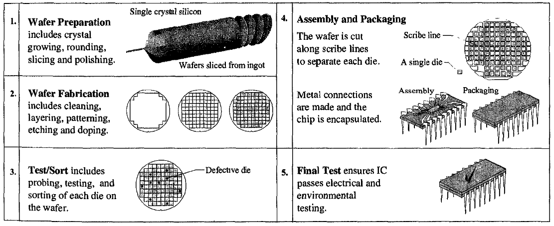 [Fig. 1-1] The process of Front-End Process and Back-End Process from wafer manufacturing
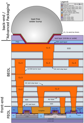 [Fig. 1-2] Categorization of processes by Front-End Process
3. Wafer Manufacturing
Manufacturing wafers is not done by electronics companies, but is very important for semiconductor performance. Wafer has semiconductor characteristics by thinly slicing semiconductor single crystals and acts as a support when the process progresses. Basically, silicon monocrystals need to be large, and the main methods used are the Czochralski (CZ) method and the flat-zone (FZ) method, and the CZ is more widely used in terms of codification.
The CZ method is to rotate the liquid silicon (melting point 1420°C) and to harden it by adding dopant to the liquid silicon, and the seed is to be single crystal silicon crystal, and the seed and liquid silicon must be rotated in opposite directions. Following the crystallinity of the seed, the liquid silicon solidifies as a single crystal forms on the seed. This method is relatively inexpensive, large diameter wafers can be produced, and silicon that is cut off and left over can be reused.
The FZ method places the polysilicon ingot where it is heated by the RF coil, moves it in one direction, and recrystallizes it to form an ingot of single crystals. Because crucible is not used, it is possible to form high-purity silicon single crystals, but it is difficult to make a large diameter, which is mainly used for Power devices requiring high-purity wafers[Fig. 1-3].
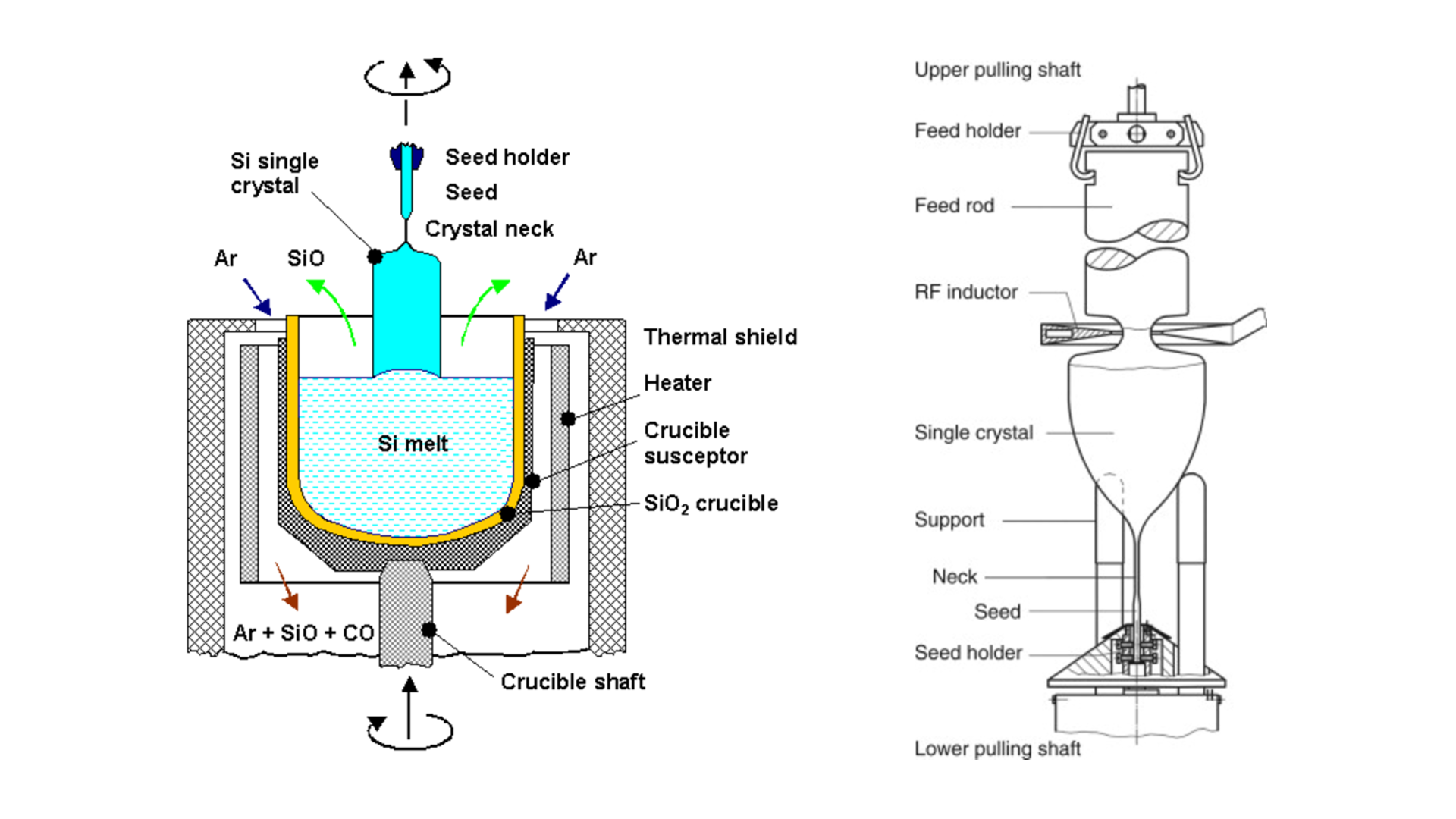 [Fig. 1-3] Float-Zone (L) and Czochralski (R) Crystal Growth
This single crystal ingot requires a thin processing process, and the process of making wafers sequentially is illustrated in [Fig. 1-4].
- Edge rounding : Insert the Wafer into the rotating milling cutter and grind the wafer edge into a round shape. If the edge is sharp, stress is concentrated and resistance to thermal stress is reduced. This causes damage to the particle, damage to the lattice.
- Lapping : The process of grinding the back of the wafer reduces wafer thickness and reduces stress.
- Wafer etching : Wet etching of silicon is carried out to remove damage generated in the previous process. (Etching Ammonium hydroxide NH4OH, Acetic acid CH3COOH, Nitric acid HNO3)
- Polishing : A process of smoothing the surface of a wafer by performing two or three polishing processes using precise slurry or polishing materials.
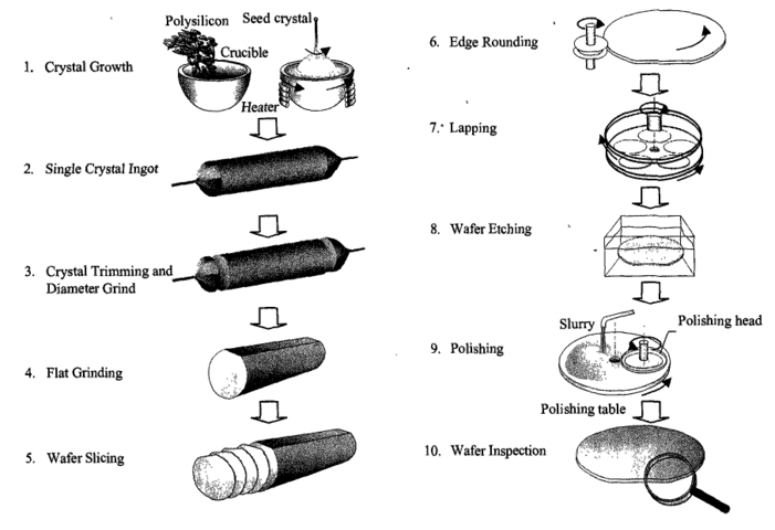 [Fig. 1-4] Wafer manufacturing process