
1. Clean Room
Semiconductor manufacturing is carried out in a very clean environment, and if these particles fall during the semiconductor manufacturing such as dust or impurities in the air, the operation may fail or stop working. Therefore, dust, humidity, and air conditioning are controlled very precisely in Fab., where semiconductor manufacturing is being carried out. They also wear white clothes, hats, and masks called smock to reduce the source of pollution falling from humans, and work with everything else covered. This enclosed space, which is controlled by particles, temperature, and humidity air pressure in the air, is called a clean room and is the most basic for securing the reliability of the process.
The unit representing the level of the clean room is class, based on the number of particles greater than 0.5um per cubic foot(ft3). The lower the class, the smaller the particle, and for high-tech semiconductor plants, it is managed less than 1 class. As we can see in [Fig. 1-5 (a)], particles are being managed from the production of silicon, especially during the process of chips. Particles are more important in high-tech processes using micro-processes because the smaller the size of the element, the greater the effect. In order to do this, particles or impurities of external air must be removed and supplied to clean rooms, but high-performance filters are used and internal air conditioning continues to be removed through filters[Fig. 1-5 (b)]. In the clean room, air is managed to circulate from top to bottom to prevent particles from floating, and to do this, air is designed to circulate by dancing holes in tiles on the floor.
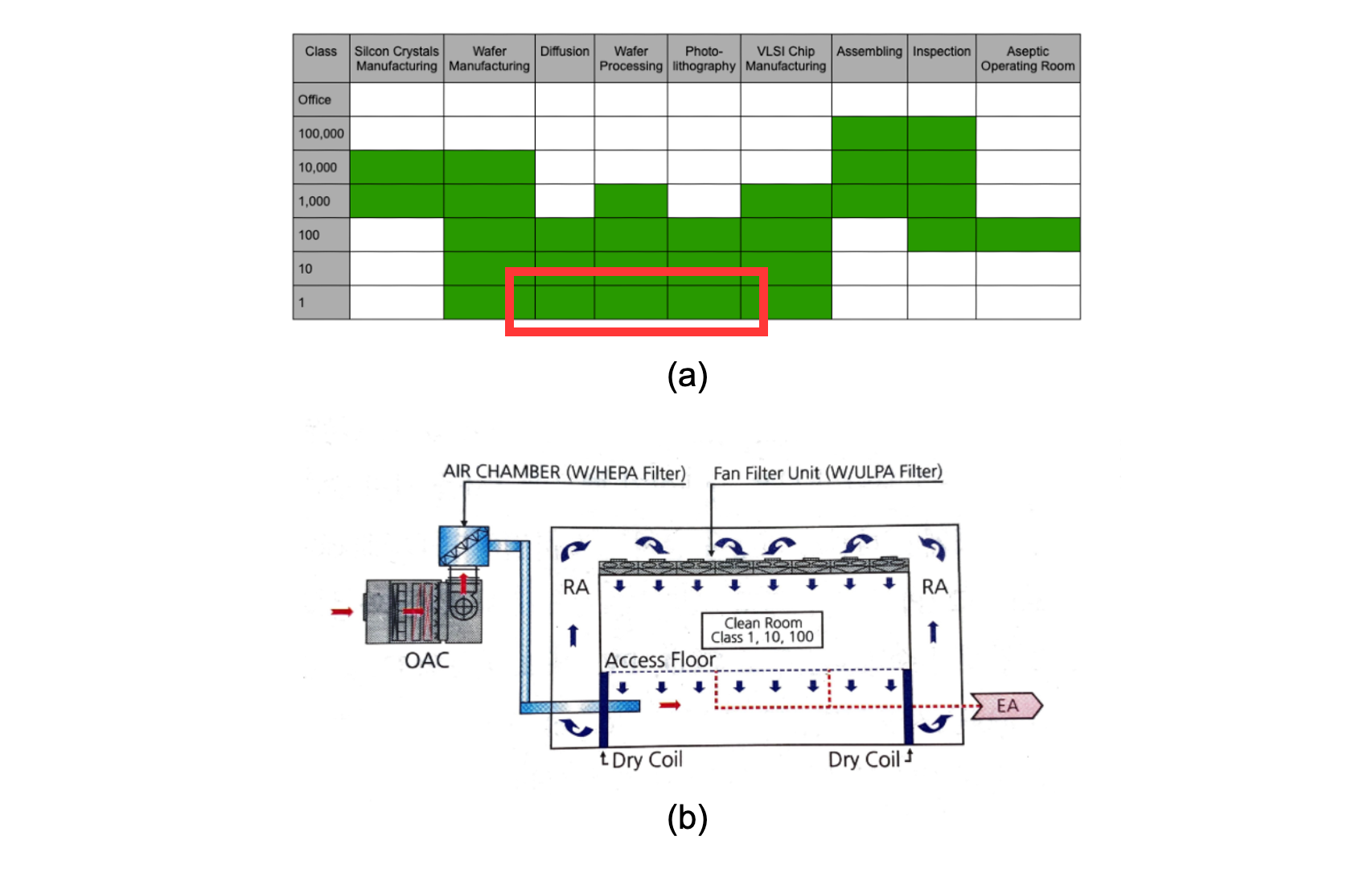 [Fig. 1-5] Cleanliness of the Clean Room
In the clean room, several facilities are aligned to perform the process, and rails designed for process automation are built above the facility so that the basic unit of the process, Lot(25 wafers), can be moved in the carrier. There is also a special space for yellow lighting, which uses light to create patterns, so yellow lighting that does not affect the process is used. This is called the Yellow Room and the process has been carried out in separate spaces in the past, but recently, the walls themselves are not good for particles, so they are only divided into areas and are all open spatially.
2. Manufacturing Facilities and Parameters
Let us understand the concept of process facilities and associated accessories placed in the clean room. Because semiconductor manufacturing is automated in facilities, if we do not understand the facilities and their components, we cannot understand the process parameters and control the process. In addition, facility engineers need to be well aware of the concept of processes as well as facilities so that they can understand the impact of their facilities on processes. This is because the process is carried out through facilities and the facilities affect the results of the process.
First, the chamber, which is the standard for process facilities, is a space where necessary parameters such as vacuum, heat, and gas can be controlled. The process is mainly carried out in the chamber, and the desired process is carried out by adjusting the relevant parameters according to the purpose in the vacuum state. Thermodynamically, the chamber can be made into a closed system so that reproducible processes can be carried out by controlling temperature and pressure. In an open system state without a chamber, even if the process parameters are identical, reproducibility may not be achieved.
At the school lab level, chambers are often used alone, but the facilities used in mass-production use cluster-type facilities to increase productivity by attaching several chambers. As shown in [Fig. 1-6 (a)], when the wafer is loaded into the facility, it is first moved to the transfer module (TM) and then entered into a chamber suitable for the purpose. TM has multiple chambers connected to it, which can increase process productivity by running the same chambers for the purpose of the facility’s process, or the in-situ process can be sequentially performed in a vacuum state by connecting different chambers. If you look at the actual cluster facilities in [Fig. 1-6 (b)], each chamber has a different shape, so the process is sequentially carried out according to the purpose through TM. If the process is listed in order, the composite process can be performed sequentially in a vacuum through the process in Loadlock TM → Chamber 1 (Process) → TM Chamber 2 (Process) → TM → … → Loadlock. Deposition processes such as CVD, PVD and ALD, and Dry etch processes use this type of cluster tool, and they are also used as in-situ processes while maintaining vacuum by connecting the dry cleaning chamber to the cluster tool.
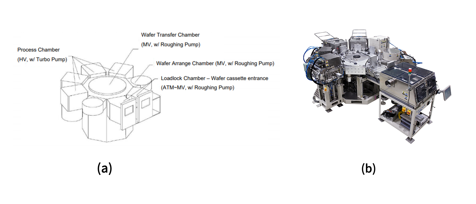 [Fig. 1-6] Manufacturing Facilities in Cluster form
However, not all facilities are built in the form of chambers. The facility is configured for the purpose of each process. In the case of a furnace for thermal process in [Fig. 1-7 (a)], heat generated from external heating lines is transferred to the wafer in the form of radiation with proper pressure and gas flow conditions in a tube made of Quartz. The tube effectively transfers the heat generated by the heating wire, making the space where the process is carried out a closed system. EUVL facilities using the optical system in [Fig. 1-7 (b)] also use optical principles to form patterns, so they are composed of purpose-built devices such as light sources and reflectors and masks that reflect light. As such, semiconductor facilities are composed of the most efficient device system for each process, and they can perform proper processes when they understand these facilities and know their impact on the process.
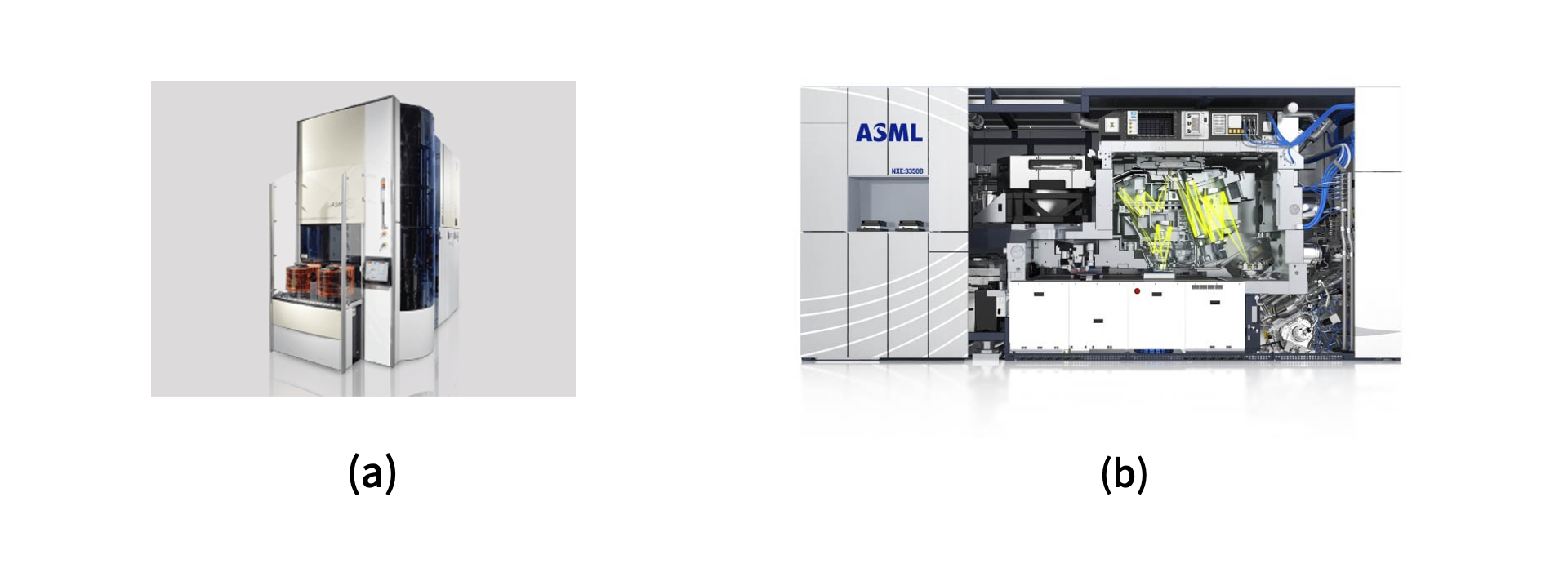 [Fig. 1-7] Utilization of facilities according to the purpose of each manufacturing
Process facility temperature to meet the conditions under which the process is carried out. Process parameters such as pressure and degree of vacuum, as well as moving or fixing wafers mechanically, should be performed. As shown in [Fig. 1-8 (a)], the function of the robot arm that allows the wafer to be properly loaded into the facility is needed, and as shown in the picture in [Fig. 1-8 (b)], the wafer is fixed in the chamber and heat is transferred. The fixing of wafers is not only when vacuum is used, but also when electrostatic chucks are used to hold them using static forces generated by applying strong voltages under the wafer. Also, since the chuck is in direct contact with the wafer, the temperature of the wafer can be adjusted directly during the process. Coolant or liquid nitrogen flows inside the chuck to control the process temperature low or to control the process temperature high by attaching heating wires.
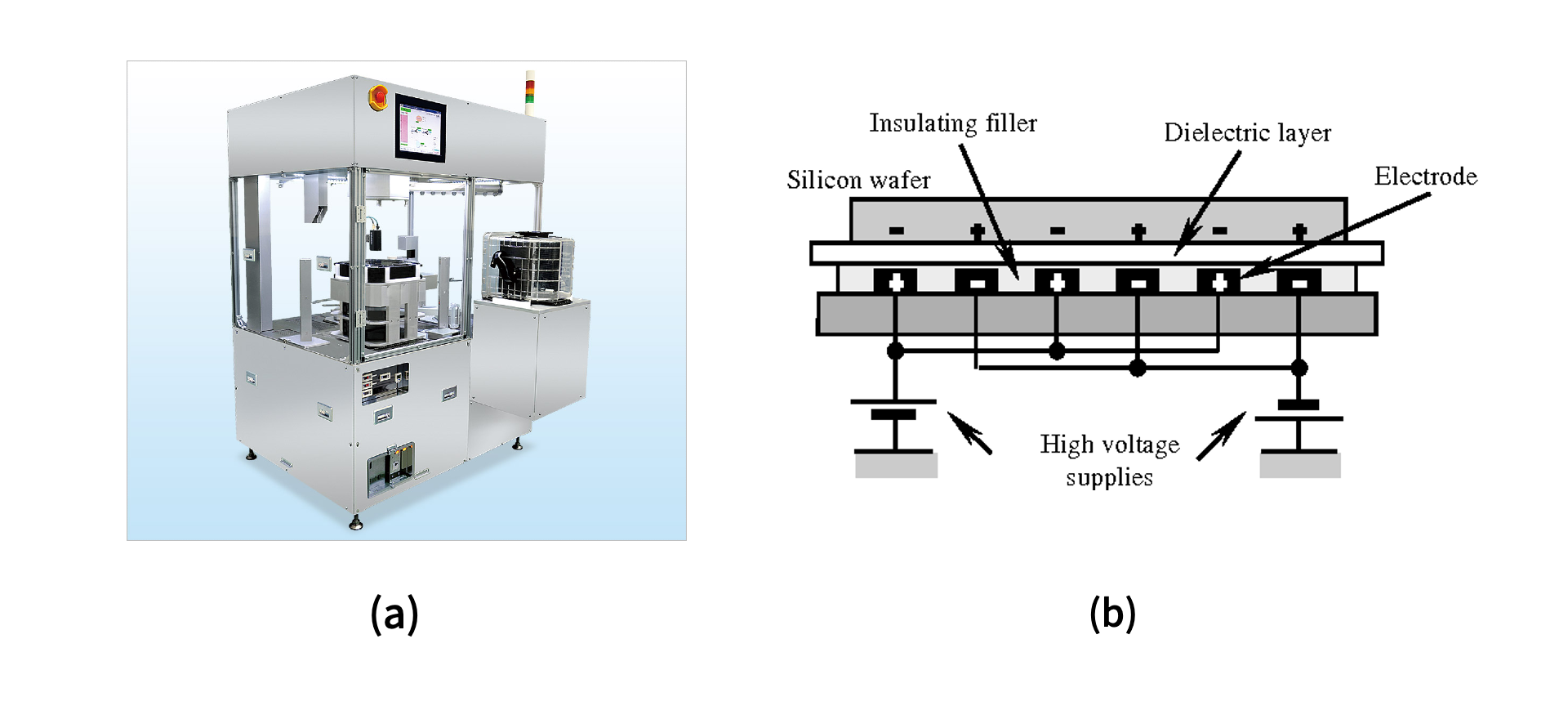 [Fig. 1-8] Wafer Transfer and Chuck
There are also various purpose-built accessories around the chamber, and let’s look at Mass Flow Controller(MFC) that measures the amount of gas supplied during the process and Scrubber for primary neutralization of gas remaining after the process. First of all, MFC is used to accurately measure the amount of gas flowing into the facility and control the process conditions. Since the MFC is a device that measures the amount of gas in the gas, if the amount of inflow is increased or decreased based on the measured value, the amount of incoming gas is adjusted by opening or closing the automated valve. As the incoming gas passes through the MFC, it passes through two parts, which are heated by a heating wire first, and the temperature of the gas changed by the heating is sensed and the amount of gas is measured. If there is a lot of gas flowing in, the temperature change is small, and if there is a small amount of gas, the temperature change is large, so the valve is opened and closed through feedback from the MFC. Scrubbers are devices that primarily neutralize or purify substances produced after the process or residual gas so that they cannot be discharged directly from the facility. Although facilities vary depending on the type of gas, they are neutralized based on chemical reactions or filtered through filters as they pass through the liquid. This primary neutralized emission gas is collected by a central purification device attached to the Fab., purged before being discharged to the outside [Fig. 1-9].
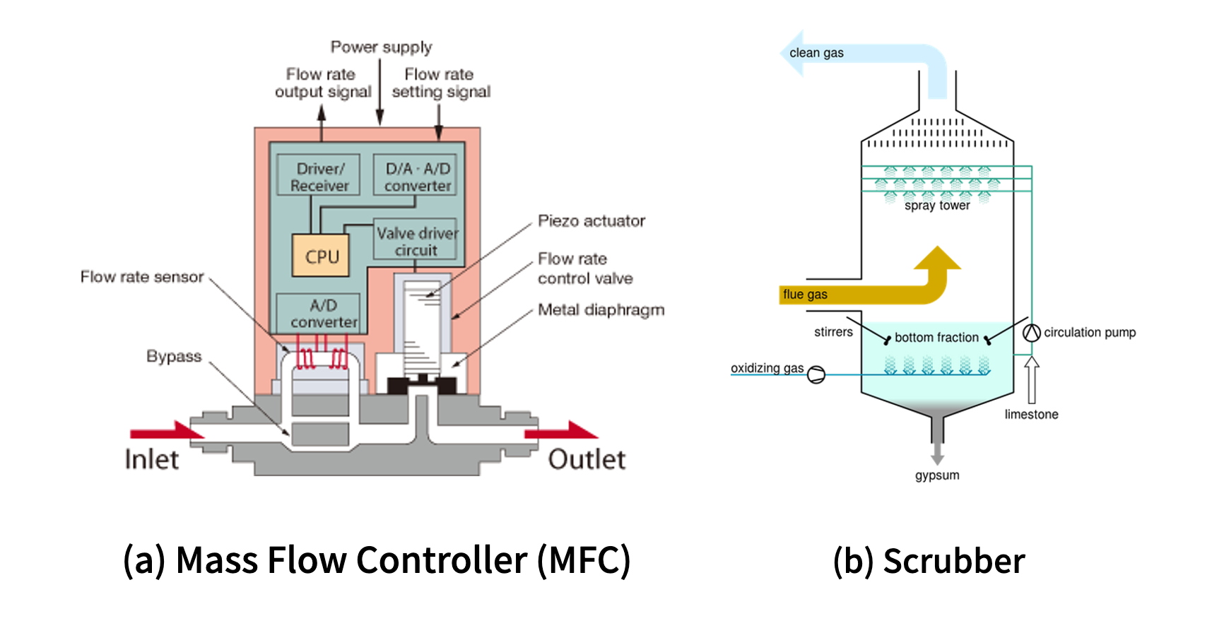 [Fig. 1-9] Critical accessories in the facility
As such, a process facility consists of a number of devices, which can be controlled to achieve the purpose of each unit process. Ultimately, the extent to which the process parameters can be adjusted can be an important point from a facility perspective, which can be made into an appropriate combination of the accessories described above. For example, for a process temperature of 400 degrees Celsius, the chuck is efficient to control the temperature with an electric heating wire, but for a process of 80 degrees Celsius, it is efficient to adjust the process temperature by flowing water or liquid.
The monitoring panel is a system created to control and monitor process conditions and facility behavior in the process. All the situations and information of the operation of the facility are expressed in one panel, so it is possible to understand what is happening in the facility at a glance. Amount injected by gas and which valve is open. This panel shows all the process-related information, such as how much vacuum is in the chamber and how much power is being supplied, and what the pump exhaust is in, so engineers can see what process is in progress.
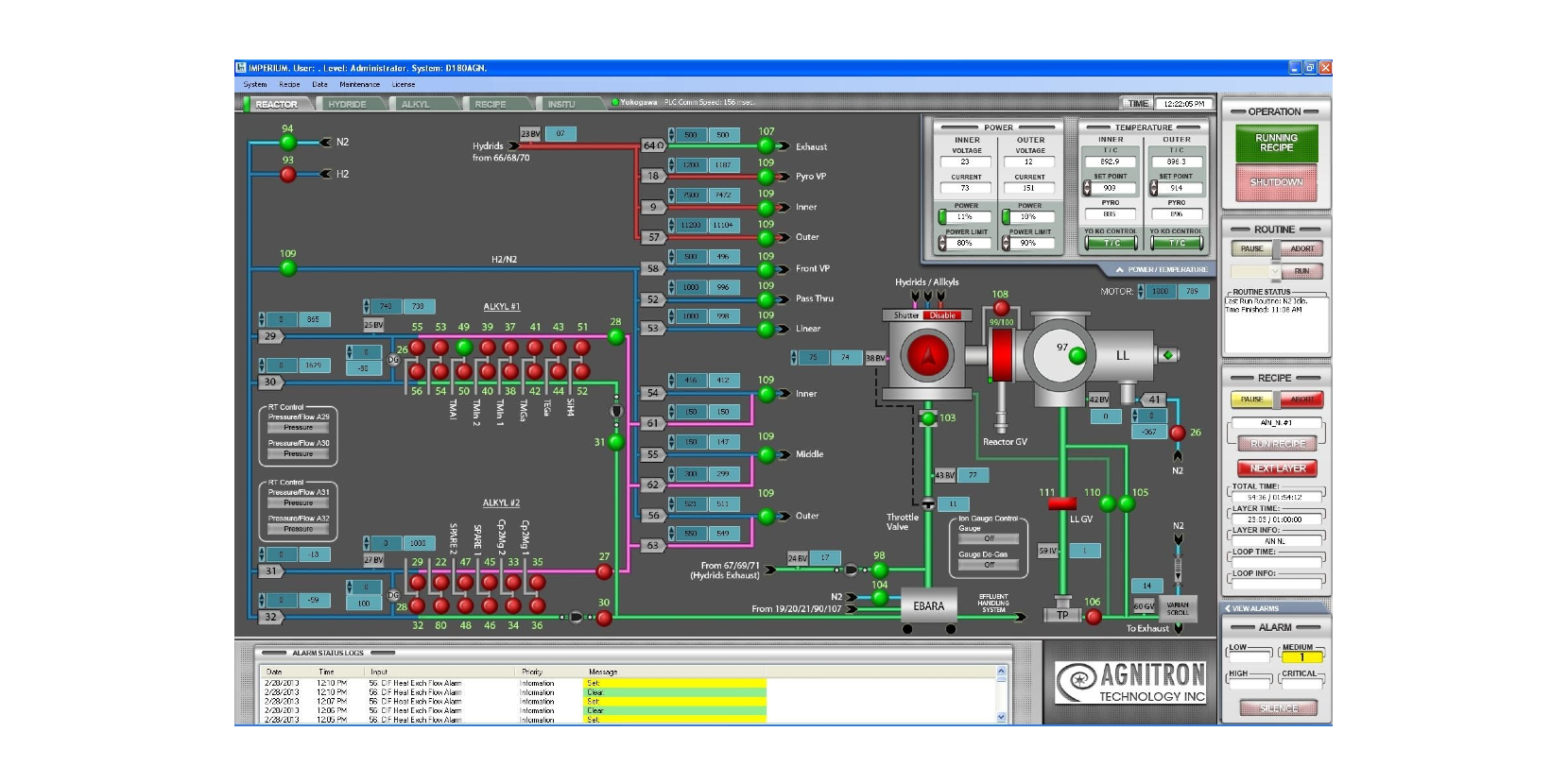 [Fig. 1-10] Facility Operation Monitoring Panel
The most important thing in semiconductor manufacturing is ‘Recipe’, which is the parameter value of each process. Just as the amount of sugar and salt can be quantified and tasted when cooking, pressure temperature and power should be controlled according to the time of the process. For example, when depositing an oxide film of 100nm, you need to know the change in the time of the process parameters, what happens when you increase the pressure, and what happens when you lower the temperature to deposit an oxide film of 100nm.